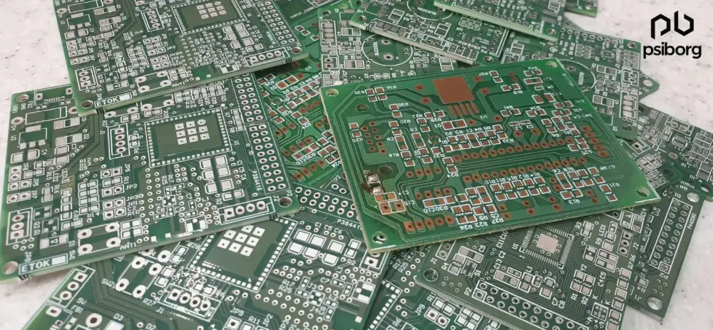
WHAT IS A PCB (PRINTED CIRCUIT BOARD) LAYOUT?
A PCB (printed circuit board) is a board that has lines and pads to connect electrical circuitry together. It is a board that brings the electronic circuits to their physical form and the components are soldered to the top, bottom, or both layers of the board. PCB design services combine the component placement and routing to define the electrical connectivity using layout software. The boards are made up of dielectric core metal and can be composed of a single layer, top and bottom layer or multiple layers of circuitry stacked together. Even small PCB Design Mistakes can lead to product failures.
As the PCB is responsible for connecting all the components with each other, making even a small error in the design can lead to a complete failure. Innovative designing tools have been able to bring down the cost of making PCBs in the last few years, but a bad PCB design can increase the cost due to the errors involved. Hence, it is important for PCB designers to avoid such PCB design issues. PCB designers need to work with ardent precision and great technical skills to make these circuit board designs.
SOME COMMON PCB DESIGN MISTAKES
Let us look in detail at some of the common mistakes made while designing a PCB board-
INCORRECT LANDING PATTERNS OF COMPONENTS
PCB design software tools include libraries of commonly used electronic components and these libraries contain both schematic symbols and PCB landing patterns and footprints. All will be fine as long as you just use the components in these libraries and according to PCB design rules, the problem starts when you want to use components not included in these libraries. When you use components, not in the library, the engineer has to manually draw the schematic symbols along with the landing patterns. It is very common for mistakes to happen while drawing these landing patterns because if the pin-to-pin spacing is off even by a millimetre, the devices are not properly soldered on the board.
THE SUB-OPTIMAL WIRELESS ANTENNA LAYOUT IS A MAJOR PCB DESIGN MISTAKE
For a wireless product, the PCB layout of the antenna is extremely important. The impedance must match the power transfer between the transceiver and the antenna to be maximum. For this two things need to be taken care of, a proper microstrip connecting the antenna and the transceiver. Generally, this step is where most PCB designers make mistakes and so they must watch very closely while doing this step.
LOCATION OF DECOUPLING CAPACITORS ON THE PCB
Critical circuit board components like decoupling capacitors need clean and stable voltage sources and for that, they are placed on the power supply rail. But for the decoupling capacitors to work best, they must be as close as to the pin requiring a stable voltage. So, for that, the power line that comes out of the power source needs to be routed so that it goes to the decoupling capacitor first and then to the pin needing a stable voltage.
It is also important to place the output capacitors for the power supply regulator as close as to the output pin of the regulator. This is important because it is necessary for optimizing stability and improving the transient response.
AVOID INSUFFICIENT POWER TRACE WIDTH WHICH IS A COMMON PCB DESIGN MISTAKE
The width of a trace is dependent on several factors like whether the trace is on the internal or the external side, thickness of the trace (copper weight), etc. and if a PCB trace has more than 500 mA running through it, the minimum width allowed will probably not be sufficient. The thickness of the trace depends on how much copper is being used in the layer. Most PCB manufacturers allow copper weights between 0.5 oz/sq. Ft. to 2.5 oz/sq. ft.
BLIND/BURIED VIAS IN THE PCB DESIGN
A through via passes through all the layers in a PCB and even if you want to connect a trace between two layers, it has to pass through the via. This can increase the size of the board because vias reduce the routing space on layers.
Blind via– It connects an external layer to an internal layer.
Buried via– It connects two internal layers. But there are restrictions as to which layers can be connected.
But unfortunately most blind/buried vias are not being manufactured. Their limitations can be understood by understanding how layers are stacked to make a board.
COPPER THICKNESS IN PCB BOARD
It is recommended to select copper with a finished thickness of 1 to 2 ounces per sq. ft. but designers generally prefer to choose 1 ounce of finished copper thickness. This may cause problems as it may fail to provide an adequate amount of plating in vias and thru-holes.
CHOOSING THE WRONG DESIGN TOOL FOR PCB DESIGNING
Choosing the correct tool for PCB design is a very important and fundamental step. It is recommended to select tools that best suit the requirements for the PCB design as choosing the wrong one can create problems like design delays and increased manufacturing costs.
TOMBSTONING IS THE PCB
Tombstoning can highly affect the PCB yields and can increase the production cost by a lot. When small passive surface mount components are soldered onto the PCB board using a reflow process it is commonly seen that one end lifts up and “tombstone”. The source of tombstoning can be incorrect landing patterns or imbalanced thermal relief to the pads. Tombstoning can be reduced by using DFM checks.
MISSING SOLDER MASK BETWEEN PADS
In small pin pinch devices that are tightly packed, it is common for there to be no solder masks between the pins. The absence of these solder masks can lead to forming of solder bridges when these fine pins are attached to the PCB during assembly.
SILVER, ACID TRAPS AND STARVED THERMALS
Small portions of copper pour when connected with large portions of the same copper pour often break during fabrication and float to other parts of the board and create unintended shorts. As silvers are now avoided in designs, the problems presented by them have been reduced in recent times by fabricator switching.
When two traces are joined together in an acute angle etching solution that is used to remove copper from the blank board can be trapped in them and these are commonly known as acid traps. Acid traps can cause traces to become disconnected from their assigned nets and leave them open-circuited. However, the issue of acid traps is less worrying now as photo-activated etching solutions are used now. It is still advised not to meet the traces at an acute angle.
When thermal relief traces that are connected to a pad are not properly connected then it is known as starved thermal. Very often the spacing between the vias passes the PCB design rules but the attached thermal reliefs interrupt and the vias become inappropriately isolated from the assigned copper pour. This problem generally happens when multiple vias are placed near each other.
LACK OF DESIGN REVIEWS
Design reviews are a very vital process in PCB designing. They involve reviewing design features, PCB functioning and interconnection of the circuits. It is always better to review the design so that you can avoid mistakes in the design.
LACK OF COMMUNICATION
Fatigue, stress, and multitasking should be avoided by circuit designers as they can affect their productivity. These can lead to miscommunication which can increase the time and money spent on making the PCB boards. Hence, it is advised to have proper communication among themselves.
FAILURE TO BACKUP YOUR WORK
Different software is used while making a successful PCB board and due to the high flexibility and speed of the software, some data might be lost easily. To avoid this problem, it is a good practice to save your data often. Create save points to ensure that even if one storage point gets corrupted, others still work fine.
METHODS TO AVOID THESE COMMON PCB DESIGN MISTAKES
There are many ways to avoid the above-mentioned mistakes in the PCB art design–
- It is necessary to follow the best practices and include design reviews.
- Utilizing the correct design tools is extremely important.
- Prototypes should be evaluated before finalizing the design
- Make sure to check the following components-
I. Design library of components
II.Mechanical features and dimensions of the board
III.Board layer stack-up configuration
IV.Mechanical parts on the board
5. All necessary files should be provided to the supplier as the design tools minimize the problems and provide complete specifications.
Also Read: IOT HARDWARE DESIGN AND DEVELOPMENT SERVICES
Want flawless PCB boards designed for your IoT product? Get in touch with us and our highly experienced engineers at PsiBorg will help you build them. With the PCB design, we also take care of PCB validation and manufacturing, making us a one-stop solution. We also specialize in providing the best IoT business development for your businesses.