
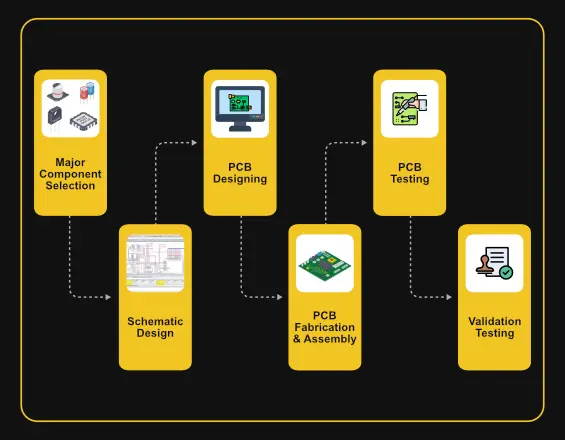
Schematic Diagram Design
We have a skilled team of embedded engineers and senior developers, so no matter how complex your project is, we can design the schematic diagram to help you reach all your project goals.

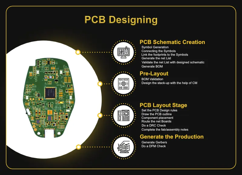
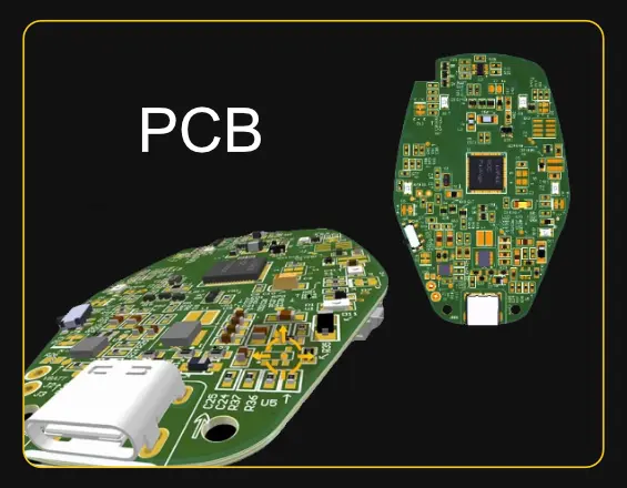
PCB Design and Layout
We have experience working with all types of PCB design software, like Altium, Cadence, Orcad, Eagle, and KiCAD, to provide you with very high-level PCB design files and full 3D CAD design output capacity.

Software Development
We can customize software functions according to your needs, whether it’s for software or an app. And help you continue to optimize in the later stages as well.

Algorithm Development
If you face any algorithmic problem, we can help you solve it. Our engineers have rich expertise in image processing, data processing, and all things related.

Industry-Leading IoT Expertise
With almost a decade of rich experience in IoT technology, we provide tailored services to various industries. Our team strives to deliver innovative and effective solutions that guarantee brilliant connectivity and automation.

End-to-End IoT Solutions – From Concept to Deployment
From the initial idea to launching your IoT project and providing continuous support, we take care of it all. You can completely focus on your business while we ensure a hassle-free experience for our clients.

Secure and Scalable Architecture
We guarantee you scalable, reliable and future-proof solutions. They are designed to provide operational efficiency, strong security, reduce downtime and align with your evolving needs.

Customized IoT Solutions for Diverse Industries
Trust us to offer tailored IoT applications that perfectly align with your specific industry requirements and deliver smart, efficient, and cost-effective solutions.


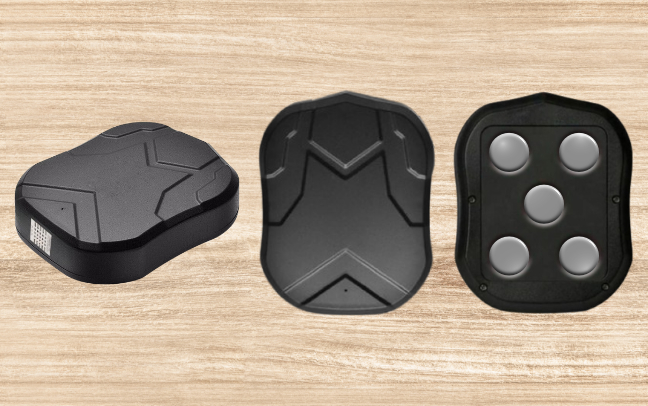
Automotive Industry: Manpower and Asset Tracking
For monitoring workforce productivity and efficiently managing valuable assets in the automotive sector, we build reliable IoT-based tracking solutions.

Mining Industry: Deployed Temperature and Humidity Monitoring
Our highly efficient IoT solutions help mining companies learn about the environmental conditions, ensure safety and comply with industry regulations.
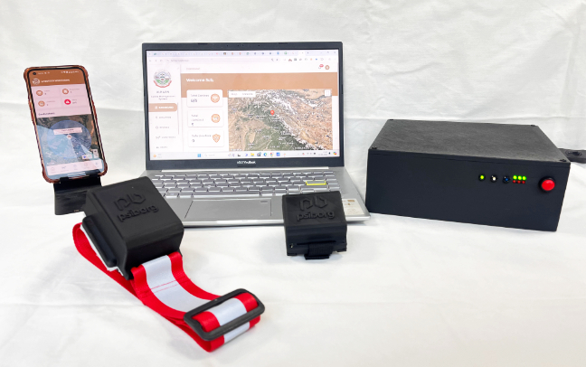
Defence: Deployed Shipment Tracking Solution
To provide security and reliability in the defense sector, we provide real-time tracking solutions that help closely monitor the movement of all critical shipments.
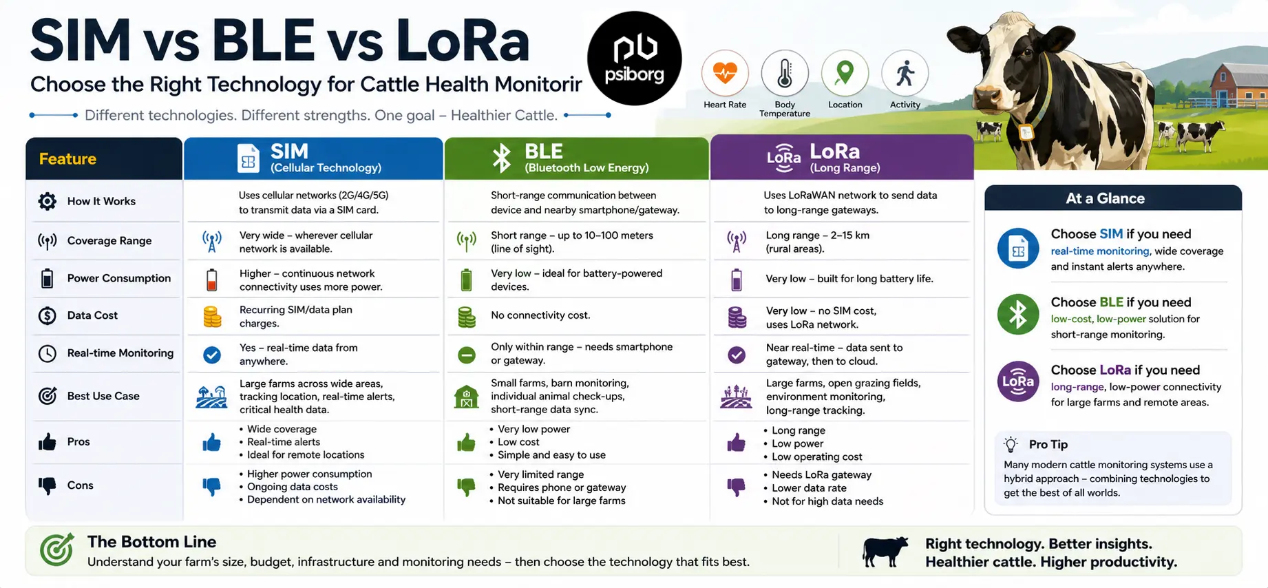
Research and Development Sector: Cattle Health Monitoring System
Researchers and farmers can track cattle health, improve productivity and detect diseases early with our IoT-enabled livestock monitoring systems.
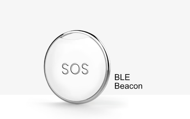
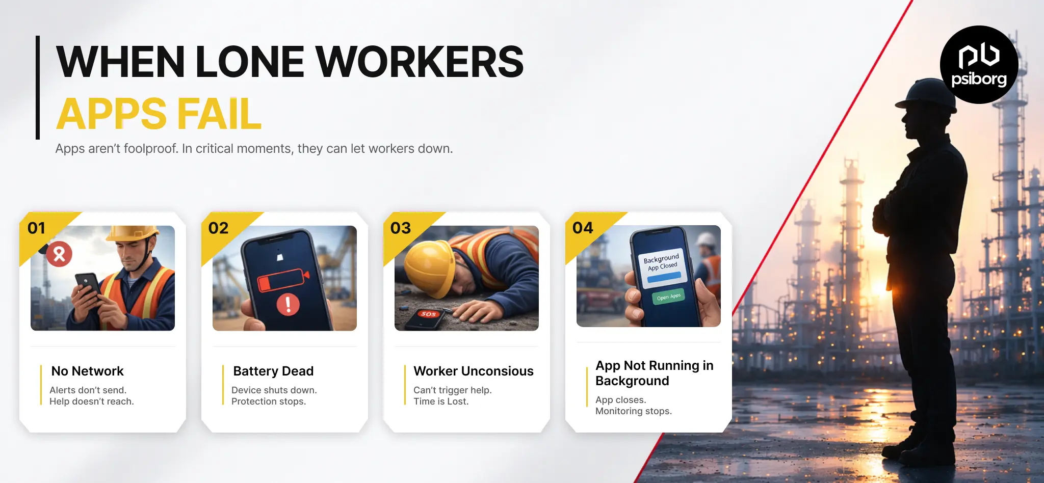
Consumer Electronics: SoS and Emergency Devices
Our IoT app development company provides efficient SoS and emergency devices that help in monitoring emergencies in real time and ensure quick responses and better safety.